
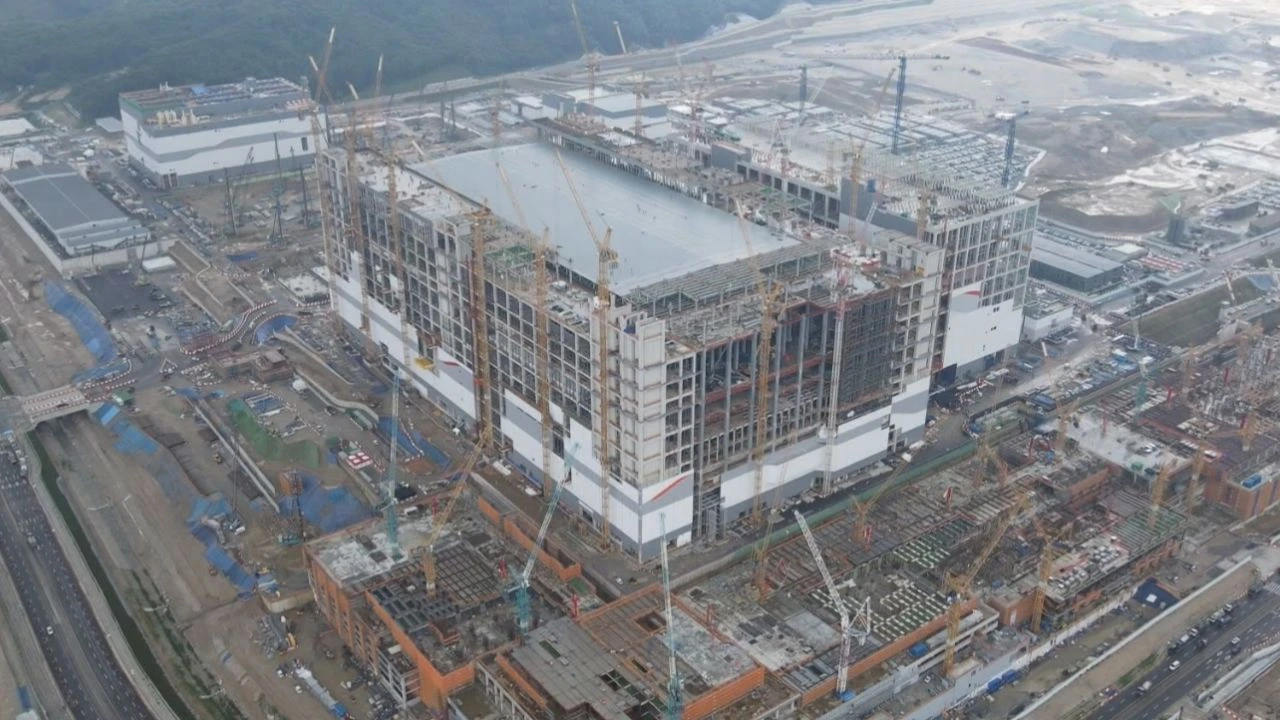
A public-private semiconductor initiative in South Korea is moving forward at the Yongin Semiconductor Cluster, south of Seoul, where SK hynix and government bodies are preparing a large-scale testing environment for chip-industry suppliers.
The project is intended to help domestic companies developing semiconductor materials, parts and production equipment evaluate their technologies before they are introduced to commercial chip lines. For smaller firms, access to production-grade tools and facilities has often been a major obstacle between a laboratory prototype and mass production.
Trinity Fab will support smaller chip suppliers
The planned testing center, known as Trinity Fab, is being built inside SK hynix’s first manufacturing plant at the Yongin Semiconductor Cluster. The cleanroom is expected to cover about 3,305 square metres and will be designed to replicate key conditions found on a working semiconductor production line.
The facility is scheduled to open in May 2027, with evaluation services expected to begin in the fourth quarter of the same year. It will provide equipment for processes including lithography, etching, deposition, cleaning, metrology and inspection.
Companies will be able to test materials and equipment with 12-inch wafers before seeking wider use in industrial manufacturing. This could reduce the need for repeated validation work after a product leaves a research setting.
| Project detail | Planned scope |
|---|---|
| Location | Yongin, Gyeonggi Province, South Korea |
| Test facility | Trinity Fab |
| Total test-bed budget | KRW 874.6 billion |
| Opening target | May 2027 |
| Planned operating start | Q4 2027 |
| Cleanroom area | 3,305 square metres |
| Equipment planned | 51 tools |
| Long-term cluster investment | More than KRW 600 trillion |
Funding combines corporate and public resources
The estimated KRW 874.6 billion cost of Trinity Fab will be supported by SK hynix, the central government, Gyeonggi Province and Yongin City. SK hynix is expected to provide the cleanroom space, technical personnel and operational expertise, while the public sector will contribute funding for the shared infrastructure.
The center is set to be run by an independent nonprofit foundation. This structure is intended to help participating suppliers protect confidential technical information while using a facility located close to an active chip fabrication site.
SK hynix has also announced a separate five-year programme worth KRW 1.4 trillion to support domestic suppliers of materials, parts and equipment. The support package includes research funding, technical cooperation and supply-chain financing.
Yongin becomes a major semiconductor manufacturing base
The wider Yongin Semiconductor Cluster is central to South Korea’s effort to reinforce its chip ecosystem amid rising demand for memory used in artificial intelligence servers and data centres.
SK hynix plans to construct four semiconductor fabrication plants at the site by 2033. Its first facility, known as Y1, is expected to begin operating its first cleanroom in early 2027. The company has advanced DRAM and high-bandwidth memory, or HBM, among the products linked to its long-term capacity plans.
Government support also includes water and power infrastructure, as chip fabrication plants require substantial and stable access to utilities. Official plans indicate that the wider industrial area will need more than 10 gigawatts of electricity by 2053 and around 1.33 million metric tons of water per day.
For smaller suppliers, the shared testing model may shorten the route from development to customer qualification. It could also give local firms a more practical way to prove that their technologies can perform under conditions similar to full-scale semiconductor manufacturing.